Osaka Metropolitan University researchers have created an adaptable and functional imaging technique that renders another typically unseen occurrence observable: surface plasmon polaritons (SPPs), light waves moving across metal surfaces. This innovative approach, published in Nano Letters, could advance the evolution of next-generation optical and plasmonic technologies.
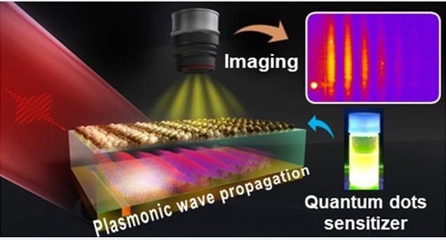 Capturing hidden light waves with quantum dots. An ultrathin layer of quantum dots acts as a light-emitting reporter, revealing invisible surface plasmon polaritons traveling along a metal–dielectric interface. The technique enables researchers to image and measure the waves with a conventional fluorescence microscope, even beneath protective dielectric coatings. Image Credit: Osaka Metropolitan University
SPPs are electromagnetic waves that propagate along the interface between a metal and a dielectric material, such as air or glass. Unlike conventional light, which spreads freely through three-dimensional space, SPPs remain tightly confined to this interface, enabling their guidance and manipulation at the nanoscale. This unique property makes them fundamental to a wide range of emerging applications, including ultrasensitive sensors, integrated optical circuits, and quantum devices.
However, tracking the propagation of SPPs has remained a significant challenge, limiting our understanding of their behavior.
Directly visualizing and characterizing their propagation, especially under realistic conditions and within complex or buried structures, has remained challenging.
Masahiro Shibuta, Study Lead Author and Associate Professor, Graduate School of Engineering, Osaka Metropolitan University
To image these waves, the research team employed a medium that is similarly tough to visualize: quantum dots, which are light-emitting semiconducting nanoparticles. By applying an exceptionally thin coating of fluorescent quantum dots to a metal surface, the scientists constructed sensitizers, substances that absorb light effectively and transfer the generated charge to a separate medium. Leveraging these nanoparticles, they produced variants that were capable of revealing SPPs in both space and time.
Upon excitation of SPPs across the coated surface with a near-infrared femtosecond laser, the propagating waves stimulated the quantum dots to emit upconversion fluorescence, a process in which multiple low-energy photons are converted into a single higher-energy photon. The resulting emission formed alternating bright and dark interference fringes that mapped the propagation of the otherwise invisible SPPs, enabling their direct visualization with a standard optical microscope under ambient laboratory conditions.
This method allows SPPs to be observed under ambient conditions, including at buried interfaces, and enables precise evaluation of their wave properties from optical images.
Masahiro Shibuta, Study Lead Author and Associate Professor, Graduate School of Engineering, Osaka Metropolitan University
By extending SPP imaging to interfaces concealed beneath comparatively thick dielectric coatings, this approach overcomes a key limitation of previous techniques, which generally required exposed metal surfaces. As a result, it broadens the applicability of the method to practical plasmonic devices operating under realistic conditions.
Beyond making the waves directly observable, the approach also enables quantitative analysis. By combining time-resolved imaging with fluorescence fringe pattern analysis, the researchers determined how dielectric films influence SPP propagation, notably changes in dispersion and propagation velocity. The experimental results closely matched theoretical predictions.
The team also found that plasmonic behavior depended on the number of quantum-dot layers deposited on the surface. This allowed them to determine the dielectric constant of the photofunctional layers, demonstrating that the approach can characterize not only SPP propagation but also the optical properties of functional nanomaterials integrated into plasmonic devices.
Our technique provides a powerful and accessible way to directly ‘see’ plasmonic waves, opening new possibilities for both fundamental studies and the design of advanced plasmonic devices.
Masahiro Shibuta, Study Lead Author and Associate Professor, Graduate School of Engineering, Osaka Metropolitan University
Moving forward, the investigators aim to broaden the method to increasingly complex plasmonic and photonic systems.
“Our ultimate goal is to establish a standard, broadly applicable platform for visualizing and controlling plasmonic phenomena, which will accelerate the development of next-generation nanophotonic and optoelectronic devices and deepen our understanding of light–matter interactions at the nanoscale,” Shibuta concluded.
Journal Reference:
Kamada, K., et al. (2026) Visualization of Internal Plasmonic Wave Photosensitized by Quantum Dots. Nano Letters. DOI:10.1021/acs.nanolett.6c02051. https://pubs.acs.org/nalefd/article/26/23/7808/5232420/Visualization-of-Internal-Plasmonic-Wave.