Researchers at ETH Zurich have developed a method that uses a single ion to detect electromagnetic fields above a surface and to create a three-dimensional map of them. In the future, this approach can be used to improve chips for quantum computers and quantum sensors.
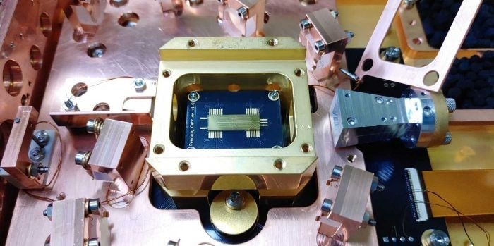 Apparatus for the experiments: The trap chip is housed in the gold-colored holder; on the chip, a single trapped ion was able to measure electromagnetic fields and create a three-dimensional map of them. Image Credit: Edgar Brucke / ETH Zurich
Single electrically charged atoms – ions – have been successfully used for some time as quantum bits in quantum computers and quantum sensors. Unlike the bulky ion traps of the early years, there are now miniaturized chips in which ions can be trapped and manipulated only a hair’s breadth above the surface of the chip. This has many advantages, but also one decisive drawback: noisy electromagnetic fields coming from the chip itself can severely impair the sensitive quantum states of the ions and hence the performance of the computer or sensor.
A team of researchers led by Jonathan Home, a professor at the Institute for Quantum Electronics at ETH Zurich, has now developed a technique that allows them to create a very precise three-dimensional map of electric and magnetic fields very close to the surface of the chip. In the future, in this way materials for chip production can be better optimized and tested for their suitability for use in quantum applications. The results of their research were recently published in the scientific journal Science Advances.
Arbitrary Movement in Three Dimensions
“Two years ago, we developed a novel chip trap that allowed to move an ion arbitrarily in three dimensions,” explains doctoral student Tobias Sägesser. Whereas in conventional traps, charged atoms are trapped by oscillating electric fields in the radio frequency range, the ETH researchers use a so-called Penning trap that is based on a combination of static electric and magnetic fields.
“This has two significant advantages,” says Shreyans Jain, also a doctoral student in Home’s group: “On the one hand, this allows us to position the ions in three dimensions, which isn’t possible using radio-frequency traps. On the other hand, the absence of oscillating fields within the trap makes it easier to detect tiny oscillating fields on the chip.”
The measurement of very small oscillating electric fields works as follows: first, the researchers use laser beams to cool a trapped beryllium ion to the point that it reaches the lowest quantum mechanical oscillation state in the trap – in other words, it effectively comes to a standstill. Then they change the electric voltages on the electrodes of the trap so that the ion moves to the desired point above the chip. “In doing so, we can vary the height above the chip from 50 micrometers up to 450 micrometers and scan an area of 200 by 200 micrometers,” says Sägesser.
Precise Field Measurement via Ion Oscillations
Once the final destination is reached, the researchers have to wait. The oscillating electric fields on the chip now continuously jolt the ion so that it starts oscillating back and forth in the trap more and more strongly. This means that its quantum mechanical oscillation state changes, which the researchers can measure using additional laser pulses after a waiting time. From this change they can then calculate the strength of the disturbing electric field.
“In this way, we have set a new record for the most sensitive measurement of an oscillating electric field in a chip trap,” says Sägesser. Within a measurement time of one second, he and his colleagues were able to detect an oscillating field with an amplitude of just 10 nanovolts per meter. For comparison: even at a distance of several kilometers the electromagnetic field of a mobile phone is still ten thousand times stronger.
The researchers can also measure static electric fields by visualizing the deflection of the ion from its resting position by a stray electric field using a microscope. To measure magnetic fields, they determine the variation of the ion’s energy levels.
A New Tool for Determining Material Properties
“For more than thirty years, researchers have tried to find out where the electric field noise close to a chip comes from,” says Home. His new method now makes it possible to measure these fields very precisely and with 3-d spatial resolution, and to compare the results to model calculations. This allows one to distinguish between different possible sources of interference. Furthermore, the Penning trap can be temporarily detached completely from all outside voltage sources, such that detrimental influences from the environment can be excluded. “Until now, one had to make certain assumptions about these influences without knowing whether they were correct,” Home explains.
Looking ahead, Home sees the new method as an additional tool for the characterization of materials. For instance, the ions can be used to scan different areas in a chip with different surface materials to determine which material creates the smallest electric fields. The manufacturing processes for the chips could also be optimized in this way.