 By Taha KhanReviewed by Lexie CornerMar 27 2024
The emergence of two-dimensional (2D) quantum materials marks a significant breakthrough in materials science, largely because of their unique structure, which is one or few atoms thick, allowing them to exhibit distinct properties valuable for specific applications. This article discusses the types, properties, applications, and promising future of 2D quantum materials.
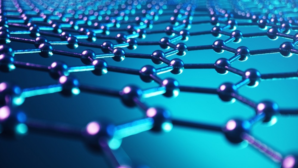
Image Credit: Rost9/Shutterstock.com
What are 2D Quantum Materials?
2D quantum materials are distinct in that, unlike 3D materials where electrons can move in all three directions, electrons are confined to two dimensions due to their atomically thin structure, leading to quantum mechanical effects.
This confinement results in unique quantum characteristics, including ferromagnetism, ferroelectricity, high-temperature superconducting, integer and fractional quantum Hall effect, quantum confinement, topological insulator, and valleytronics physics.1 Their high surface area-to-volume ratio also endows them with exceptional surface properties, impacting phenomena like catalysis and adsorption.
Types and Properties of 2D Quantum Materials
There are numerous types of 2D quantum materials, each exhibiting unique properties beneficial for specific applications. Graphene is among the most prominent types—a 2D material made of a single layer of carbon atoms arranged in a honeycomb lattice. It stands out for its exceptional electrical conductivity, high mechanical strength, and unique optical properties.
For instance, graphene's band structure enables it to absorb light of any quantum energy,2 making it suitable for use in photonics as part of high-resolution imaging systems, optoelectronic transceivers, or as a detector of light.3
Transition Metal Dichalcogenides (TMDCs) are another type of 2D quantum material. They are composed of various combinations of transition metals, like molybdenum or tungsten, and chalcogens, such as sulfur or selenium. These materials exhibit a wide range of properties, including semiconducting behavior, strong light-matter interaction, and potential for superconductivity.4
Other 2D quantum materials, including Hexagonal Boron Nitride (h-BN), Phosphorene, Silicene, Germanene, and Stanene, also exhibit various properties, such as electrical conductivity, strength, flexibility, and optical characteristics. These attributes render them valuable in a variety of applications.
Transformative Applications of 2D Quantum Materials
The unique properties of 2D quantum materials enable their application across a wide range of industries, including electronics, spintronics, energy storage, and quantum computing. For example, a recent study highlighted graphene's potential in flexible electronics due to its exceptional mechanical, thermal, electrical, and optical properties, making it an ideal candidate for flexible electronic (FE) devices.5
This research focused on graphene's role in flexible thin film transistors (TFTs), showcasing its ability to surpass traditional semiconductor materials in terms of carrier mobility and heat dissipation. Despite challenges like zero bandgap and complex fabrication processes, graphene demonstrates promise as a semiconductor material.
Graphene's applications extend to flexible transparent conductive materials, electrode materials for flexible lithium batteries, and membrane materials for flexible batteries, highlighting its versatility and significance in advancing flexible electronics technology.5
Certain 2D materials are also recognized for their suitability in constructing quantum computers, as their unique electronic structures can be harnessed to create robust qubits. Similarly, TMDCs, including WSe2, WS2, MoSe2, and MoS2, are perfect for high-efficiency photodetectors due to their charge transport capabilities and bandgaps in the optical or near-infrared region. This makes them promising materials for next-generation sensors, biomedical devices, transistors, and solar cells.6
Challenges and Opportunities
Before 2D quantum materials can achieve widespread practical applications, they must overcome specific challenges. Challenges include synthesizing high-quality, large-scale 2D materials and ensuring their stability and the retention of desired properties during device integration. Nevertheless, ongoing research efforts are actively addressing these challenges.
A notable advancement came from a 2020 study that addressed the scalability issues of 2D materials. Researchers introduced a scalable method to precisely control the thickness of 2D materials, a critical issue for their integration into functional devices. This method, involving a simple oxidation/etching process, selectively removes the top layers of various 2D materials like germanium disulfide (GeS2), germanium sulfide (GeS), and germanium arsenide (GeAs).7
Through experimentation and simulations, the study demonstrated layer-by-layer thinning, which is crucial for controlling material properties. The method, adaptable to different 2D materials with suitable reagent choices, offers a solution to scalability issues previously encountered with top-down approaches. When combined with lithography, this method also allows for precise patterning, enhancing its utility in device fabrication.
This advancement provides a significant contribution to the utilization of 2D materials in electronics and optoelectronics.7
Future Outlooks
2D quantum materials represent a frontier in materials science, offering diverse properties and potential for transformative technological applications. Quantum computing materials, such as graphene, TMDCs, and other 2D materials, exhibit remarkable properties, making them invaluable for various quantum applications.
Despite challenges in scalability, synthesis, and integration, recent research advancements offer promising solutions. Scalable methods for controlling material7 show potential for large-scale production and device integration.
To fully realize the transformative potential of these materials, continued research, collaboration, and investment in the field are critical.
More from AZoQuantum: Exploring Exciton 'Holes': Novel Insights from Electron Spectroscopy
References and Further Reading
- Liu, J., Ding, Y., Zeng, M., Fu, L. (2022). Chemical insights into two-dimensional quantum materials. Matter. doi.org/10.1016/j.matt.2022.05.034
- Lemme, M. C., Akinwande, D., Huyghebaert, C., Stampfer, C. (2022). 2D materials for future heterogeneous electronics. Nature communications. doi.org/10.1038/s41467-022-29001-4
- Graphenea. (no date). Photonic applications of graphene. [Online] Graphenea. Available at: https://www.graphenea.com/blogs/graphene-news/photonic-applications-of-graphene (Accessed on 26 March 2024).
- Wang, Q. H., Kalantar-Zadeh, K., Kis, A., Coleman, J. N., Strano, MS. (2012). Electronics and optoelectronics of two-dimensional transition metal dichalcogenides. Nature nanotechnology. doi.org/10.1038/nnano.2012.193
- Chen, Y. (2023). Graphene and its application in flexible electronics. ACE. doi.org/10.54254/2755-2721/7/20230430
- James Singh, K., et al. (2021). Recent advances in two-dimensional quantum dots and their applications. Nanomaterials. doi.org/10.3390%2Fnano11061549
- Sun, J., Giorgi, G., Palummo, M., Sutter, P., Passacantando, M., Camilli, L. (2020). A scalable method for thickness and lateral engineering of 2D materials. ACS Nano. doi.org/10.1021/acsnano.0c00836
Disclaimer: The views expressed here are those of the author expressed in their private capacity and do not necessarily represent the views of AZoM.com Limited T/A AZoNetwork the owner and operator of this website. This disclaimer forms part of the Terms and conditions of use of this website.