Semiconductor chips serve as the foundation of 21st-century digital innovation and the global economy. The rapid growth of the AI industry, progress in quantum computing, and the increasing demand for faster, more efficient computing have significantly driven the need for high-performance chips.
However, detecting failures and inspecting semiconductor chips for defects remains a critical yet highly complex challenge. In this context, the integration of quantum imaging, machine learning–based next-generation imaging technologies, and data analytics–driven inspection and maintenance approaches can strengthen productivity, enhance reliability, and support more sustainable manufacturing practices.1
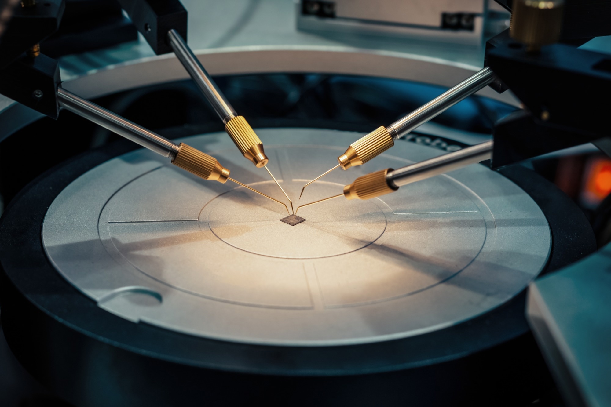
Image Credit: Nordroden/Shutterstock.com
The Challenge of Nanoscale Defect Detection
The photolithographic processing during the manufacturing of semiconductor chips leads to various nanoscale defects, particularly during EUV pattering. The continual reduction in semiconductor chip dimensions, combined with the precise nanoscale patterning required for advanced AI chips, results in sub-nanometer defects that can be easily overlooked during inspection and defect detection processes.
The traditionally used Scanning Electron Microscopy (SEM) consumes a lot of time and resources, making it ineffective for modern sub-nanometer defects, and a financially inefficient option.2 Atomic Force Microscopy (AFM) has also been proven to be less impactful than SEM for defect detection at the nano-scale, while being more expensive than traditional systems.
With the recent shift towards EUV lithography, the inspection time has increased massively as this extremely precise manufacturing process incurs highly miniaturized stochastic defects. The low depth-of-focus (DOF) of the electronic beam for defect detection is forcing the manufacturing of thinner resists and innovative underlayers, which prove to be a major hurdle in defect detection.3 The EUV sources and optics-based defect detection and inspection units are very expensive, with complete semiconductor wafer inspection using EUV beams being impractical even today.4
No time now? Download the PDF for later
Quantum Imaging: The Next Frontier
Experts view quantum imaging as a highly advanced technology capable of addressing the limitations of conventional semiconductor defect detection methods. These imaging techniques offer significant advantages: they do not damage semiconductor wafers, provide enhanced resolution and sensitivity, and generate far more detailed images compared to traditional approaches.
Quantum imaging techniques that make use of quantum entanglement and quantum correlations enable precise detection of sub-nanometer defects during semiconductor chip manufacturing. By harnessing quantum states of light, researchers can overcome classical limitations related to spatial resolution, positioning quantum imaging as a strong candidate for advanced semiconductor defect detection.
Quantum Ghost Imaging (QGI) for Semiconductors
QGI is an intriguing and innovative imaging method utilizing the correlation between photon pairs for constructing images at the nanometer level. During QGI, the photon pairs generated by spontaneous parametric down-conversion (SPDC) in a non-linear crystal enable us to capture nanometer-level defects in semiconductors while satisfying energy and momentum conservation. Additionally, QGI has also been excelling in Near Infrared (NIR) low-light imaging, surpassing traditional imaging techniques.5
Quantum Sensing with Spin Defects for Semiconductors
Solid-state defects allow for quantum sensing at room temperature without the need for specialized equipment and a vacuum. The integration of quantum sensing with imaging equipment allows for unmatched sensitivity, with diamond NV centers being studied extensively.
Defect-based quantum sensing is emerging as a leading approach in semiconductor wafer inspection, particularly for analyzing complex circuitry and three-dimensional compound structures. In addition, diamond NV centers have demonstrated strong potential as non-invasive, super-resolution tools for defect detection and for inspecting modern semiconductors, especially in the study of their magnetic and electrical properties.
A few key applications of quantum sensing in semiconductor device inspection and defect diagnosis include individual bit detection in modern magnetic random-access memory (MRAM), and analyzing and regulating current flow in modern 3D integrated circuit (IC) based semiconductor devices by inspecting the architecture, and removing manufacturing defects.6
Next-Generation Imaging Technologies
Experts are also utilizing digital technologies like ultrafast lasers and Machine Learning (ML) tools for developing extremely efficient imaging techniques for semiconductor devices.
Laser-Based Imaging for Semiconductor Defect Detection
Laser-based imaging techniques are becoming essential for semiconductor defect detection, maximizing the yield of chips during manufacturing. Laser-based methods have much superior and higher throughput, and imaging efficiency in non-contact mode, making ultrafast laser-based imaging techniques ideal for inline defect inspection.
Experts have developed an exceptionally sensitive laser-based quantitative phase imaging system integrated with an epi-illumination diffraction phase microscope, making it well suited for semiconductor and silicon wafer defect detection. The system incorporates a frequency-doubled Nd:YAG 532 nm solid-state laser, and in-plane imaging was carried out on a 22 nm node intentional defect array (IDA) wafer-based semiconductor device.
The imaging system proved to be immune to vibrational noise and enabled the reconstruction of amplitude and phase images in a single instance. The imaging system efficiently detected 20 nm * 100 nm * 110 nm defects.
The experts also developed a second, much more powerful system, using a 405nm diode laser, which was used to analyze and provide images of a 9nm node IDA wafer. This powerful system successfully provided images of 5 nm by 90 nm by 35 nm defects in the densely patterned semiconductor wafer.7 This proves that ultra-fast laser-based imaging is becoming crucial for identifying defects in modern nm-scale semiconductor chips.
AI-Powered Next-Gen Semiconductor Metrology
The three-dimensional semiconductor architecture pushing us into the sub-nanometer era has rendered classical metrology techniques ineffective. Experts have integrated AI-based algorithms like Neural Networks (NNs) for precise optical metrology. Surrogate models are being developed using NNs, enabling the nonlinear mapping of nanoscale geometric parameters and the optical responses using data-driven modeling. The NN-based model is highly efficient, enabling non-destructive and real-time defect monitoring, leading to an improvement of around 300 times compared to traditional optical imaging techniques.8
Industry Leaders and Startups
Industrial leaders and startups are focusing on the development and adoption of these next-gen imaging systems for significantly increasing the yield of semiconductor chips during manufacturing.
IBM has developed a vision transformer (ViT) NN for automatic defect classification in semiconductor images taken using SEM. The NN achieved an accuracy of over 90% while analyzing over 7500 images of a 300mm semiconductor wafer.9
Furthermore, IBM has developed IBM Maximo, an AI-powered tool which accelerated the process of defect detection, massively boosting productivity and cutting down costs during semiconductor chip manufacturing.10
Another critical development is the acquisition of the startup Canopus AI by Siemens, revolutionizing the AI-based metrology sector by innovating the computational and AI-driven defect detection processes. The integration of the AI-system has led to a much more stable, efficient, and productive end-to-end EDA digital system that accelerates the yield by reducing the defect detection time.11
Startups like EuQlid are also focusing on utilizing quantum sensing mechanisms for detecting nanoscale defects in semiconductor interconnects, and a 3D semiconductor sandwich architecture with unmatched efficiency and accuracy. The EuQlid quantum sensing platform, QuMRI, enables precise mapping of current flow in deep semiconductor interconnects in a contactless manner, enabling about 100 times faster detection of defects in modern semiconductor chips.12 The interest of tech giants and the emergence of various startups all point towards the success and bright future of next-gen imaging systems for semiconductor inspection.
What’s Next?
While next-gen imaging systems and quantum-based technologies feel like the perfect solution, certain technical and financial challenges are hindering their widespread adoption. Cost-effective automated next-gen imaging systems for semiconductor chip defect detection haven’t been achieved, as ensuring compatibility of novel systems with existing infrastructure, and the cost of developing innovative components is very high compared to conventional methods.
Currently, the development and operational costs associated with these modern imaging systems are causing various manufacturers to stick to tested conventional methods, as they don’t require any drastic changes to the manufacturing processes.
Furthermore, several modern imaging systems have been characterized with nuisance detections and false alarms due to different reasons, such as edge-of-field effects. This leads to a big blow to the trust of manufacturers in modern imaging systems, with various companies still waiting for the technology to mature and become cost-efficient.
The semiconductor manufacturing industry is flourishing continuously, with annual sales expected to reach US$ 2 trillion by 2036.13 With the massive increase in demand for powerful AI chips, the future of semiconductor inspection involves the integration of quantum imaging systems with ML-powered data-based algorithms, enabling real-time, faster defect detection. The constant innovation in E-beam detection technologies, quantum imaging systems, ultra-fast laser-based defect detection systems, and AI-powered metrology systems ensures that the imaging-based semiconductor defect detection instrument industry will see a massive boom in the next decade.
Keep this article with you - download the PDF here
Further Reading
- Park, J., Yoo, B., Baek, S.Y., Youn, C., Kim, S., Kim, D., Roh, S., Park, S.J., Kim, J., Lee, C. and Choi, C. (2025). Advancing Condition-Based Maintenance in the Semiconductor Industry: Innovations, Challenges and Future Directions for Predictive Maintenance. IEEE Transactions on Semiconductor Manufacturing, 1–1. DOI: 10.1109/tsm.2025.3530964. https://ieeexplore.ieee.org/abstract/document/10844902
- Shinde, P.P., Pai, P.P., Adiga, S.P., Subramanya Mayya, K., Seo, Y., Hwang, M., Go, H. and Park, C. (2025). Defect detection in photolithographic patterns using deep learning models trained on synthetic data. Heliyon. 11(10). 43377. DOI: 10.1016/j.heliyon.2025.e43377. https://www.sciencedirect.com/science/article/pii/S240584402501761X
- Chen, Y.-L., Deforce, J., Ridder, V.D., Dey, B., Blanco, V.M., Halder, S. and Leray, P. (2024). Towards improved semiconductor defect inspection for high-NA EUVL based on SEMI-SuperYOLO-NAS. Ghent University Academic Bibliography (Ghent University). 30. DOI: 10.1117/12.3010940. https://www.spiedigitallibrary.org/conference-proceedings-of-spie/12955/129550W/Towards-improved-semiconductor-defect-inspection-for-high-NA-EUVL-based/10.1117/12.3010940.short
- Averroes.ai. (2022). Averroes. [online] Available at: https://averroes.ai/whitepaper/euv-defect-detection-challenges-and-ai-solutions?utm_source=copilot.com [Accessed 06 Feb. 2026].
- Ryan, D.P., Mos, P., Lin, Y., Bruschini, C., Charbon, E. and Werner, J.H. (2025). Time-resolved detectors for quantum ghost imaging. The European Physical Journal Plus. 140(6). DOI: 10.1140/epjp/s13360-025-06393-y. https://link.springer.com/article/10.1140/epjp/s13360-025-06393-y
- Kim, K., Moon, J.S., Lee, D., Lee, J.H., Lee, Y., Park, C., Chung, J., Lee, D. and Kim, J.-H. (2025). Quantum sensing with spin defects: principles, progress, and prospects for use cases. Advanced Photonics,. 7(06). DOI: 10.1117/1.ap.7.6.064002. https://www.spiedigitallibrary.org/journals/advanced-photonics/volume-7/issue-06/064002/Quantum-sensing-with-spin-defects--principles-progress-and-prospects/10.1117/1.AP.7.6.064002.full
- Zhou, R., Edwards, C., Popescu, G. and Goddard, L. (2015). Semiconductor defect metrology using laser-based quantitative phase imaging. SPIE Proceedings, 9336. 93361I.. DOI: 10.1117/12.2078329. https://www.spiedigitallibrary.org/conference-proceedings-of-spie/9336/1/Semiconductor-defect-metrology-using-laser-based-quantitative-phase-imaging/10.1117/12.2078329.full
- Xu, W., Zhang, H., Ji, L. and Li, Z. (2025). AI-Powered Next-Generation Technology for Semiconductor Optical Metrology: A Review. Micromachines. 16(8), 838–838. DOI: 10.3390/mi16080838. https://www.mdpi.com/2072-666X/16/8/838
- Huang, C.-F., Sieg, K., Karlinsky, L., Flores, N., Sheraw, R. and Zhang, X. (2025). Semiconductor SEM Image Defect Classification Using Supervised and Semi-Supervised Learning with Vision Transformers. [online] IBM Research. Available at: https://research.ibm.com/publications/semiconductor-sem-image-defect-classification-using-supervised-and-semi-supervised-learning-with-vision-transformers [Accessed 11 Feb. 2026].
- IBM Mediacenter. (2019). IBM Maximo: accelerate defect detection with AI-powered visual inspection software. [online] Available at: https://mediacenter.ibm.com/media/IBM+MaximoA+accelerate+defect+detection+with+AI-powered+visual+inspection+software/1_zu2t8b6c [Accessed 11 Feb. 2026].
- Siemens Digital Industries Software. (2026). Siemens acquires Canopus AI. [online] Available at: https://news.siemens.com/en-us/siemens-acquires-canopus-ai/ [Accessed 12 Feb. 2026].
- Choi, C.Q. (2025). Quantum Sensor Startup Seeks Flaws in 3D Chips. [online] IEEE Spectrum. Available at: https://spectrum.ieee.org/quantum-sensors-2674296517 [Accessed 12 Feb. 2026].
- Deloitte (2025). 2025 global semiconductor industry outlook. [online] Deloitte Insights. Available at: https://www.deloitte.com/us/en/insights/industry/technology/technology-media-telecom-outlooks/semiconductor-industry-outlook.html. [Accessed 14 Feb, 2026].
Disclaimer: The views expressed here are those of the author expressed in their private capacity and do not necessarily represent the views of AZoM.com Limited T/A AZoNetwork the owner and operator of this website. This disclaimer forms part of the Terms and conditions of use of this website.