Chips are becoming more advanced, but they are still, in most cases, made by stacking layers one on another. Scientists at the University of Twente created a three-dimensional structure that includes a functioning superconducting device mounted on top. The results are published in Physical Review Applied.
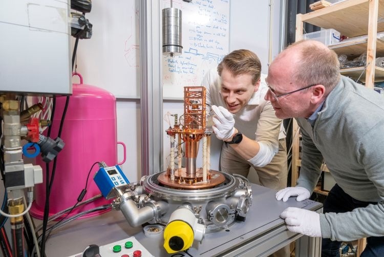 Image Credit: University of Twente
The device is pyramid-shaped and stands several micrometers tall. At its apex is a superconducting ring a few hundred nanometers across, designed to measure magnetic fields at the highest sensitivity allowed by physics.
Quantum materials can behave in ways ordinary materials cannot. They can carry current with no loss, or they can conduct current only along their outer edge while the interior remains insulating. Future quantum computers and quantum sensors are expected to rely on materials like these. To improve them, researchers need a precise way to map currents and magnetic fields at the nanoscale.
This type of sensor is known as a SQUID (superconducting quantum interference device): a superconducting ring built to detect extremely small changes in magnetic fields. The main challenge is proximity, because magnetic fields decay rapidly with distance, so the sensor has to sit very close to the material under study.
If such a ring is positioned flat across the plane of a chip, the rest of the chip raises it several micrometers away from the material. That is where fine detail is no longer captured. The University of Twente has worked for years on scanning SQUID microscopy, using it to map the magnetism of surfaces.
That is why we put the sensor on a pyramid. On top of that pyramid the sensor can be brought right up to the material we want to look at, with nothing else in the way. That lets us image magnetism at the scale where quantum materials do their work.
Hans Hilgenkamp, University of Twente
This approach can enable new materials with distinctive functionality. Through the Gravitation program QuMat, Twente develops the instruments that it and its partners use to measure quantum materials and continue advancing them.
Two Twente Specialisms on a Single Point
The pyramid is not built up. Instead, researchers start by hollowing it out from a single piece of silicon, the same base material used to make computer chips. Using a liquid, the team removes material by carving pits shaped like an upside-down pyramid. Over each pit, they place an ultra-thin film of a glass-like material, which becomes slightly thicker at the sharp edges. After taking that film away again, the remaining material is left only in those edges.
What remains is a framework of extremely fine wires, placed precisely along the pyramid’s ribs. This fabrication approach, known as corner lithography, was developed by Edin Sarajlic, Erwin Berenschot, and Niels Tas in the University of Twente’s Mesoscale Chemical Systems group, which specializes in building three-dimensional nanoscale structures.
Researchers then remove the surrounding silicon, leaving the pyramid standing at the end of a thin, flexible arm. Under a microscope, that arm scans across the surface. Much like a record player’s needle tracking a groove, it follows the contours of the sample.
Next, a layer of niobium is deposited over the wires. Niobium becomes superconducting at very low temperatures. In the final step, a focused beam of charged particles cuts two narrow constrictions into the ring at the apex, completing the sensor.
We come from superconductivity, our colleagues from 3D nanofabrication. Both techniques already worked well. Combine them and you get three-dimensional devices with unmatched possibilities.
Thijs Roskamp, PhD Candidate and Study First Author, University of Twente
For decades, the chip industry primarily worked in a flat plane. Layer-by-layer stacking has become common, but fully three-dimensional structures that also contain working electronics inside remain uncommon. This sensor demonstrates that such designs are possible.
Still Measuring Where Superconductivity Normally Gives Out
Research on quantum materials often uses strong magnetic fields. That creates a problem for a superconducting sensor, since a strong magnetic field is exactly what breaks superconductivity. As a result, the most sensitive sensors stop working precisely when they are most needed. The Twente sensor continues to operate above 1 tesla, about twenty thousand times the Earth’s magnetic field.
There is also another benefit. The frame at the tip has four wires, but only two are needed for the measurement. The remaining two serve as extra connections. This lets researchers control the sensor directly from the tip and adjust its sensitivity while it scans.
Our sensor has four connections from the start. We use two to measure and the other two stay free. We can add functions to those without having to make the sensor all over again.
Thijs Roskamp, PhD Candidate and Study First Author, University of Twente
From Handwork to a Whole Wafer
Other teams are working to create SQUID-on-tip sensors like this, but so far the process is still mostly manual. A specialist first draws a glass tube into a fine needle and then deposits superconductor on it over several steps. The approach works, but it produces one sensor at a time, with limited reproducibility and little ability to add additional features at the tip.
At the MESA+ NanoLab in Twente, the sensor is made using the same steps as the chip industry. The fabrication is done across an entire silicon wafer at once, producing hundreds of pyramids side by side during a single production run. Between 80 and 90% of the tips on the wafer are usable. The ring size can also be adjusted. By altering the hollowed-out pit, the researchers produced sensors ranging from several micrometers down to about 100 nanometers.
Colleagues from Bruker contributed to the work. Bruker is a manufacturer of scanning microscopes based in Enschede and operates within the MESA+ NanoLab. This significantly reduces the distance between an experimental setup and a sensor that other laboratories can order.
“Our role in QuMat is to build tools,” says Hilgenkamp. “We develop the sensors that let us measure remarkable quantum materials together with others in the consortium.”
The research originates from QuMat, Materials for the Quantum Age, a ten-year research program funded by the Dutch Ministry of Education, Culture and Science and led out of Utrecht University. Twente is a major partner in the consortium, with multiple projects focused on developing and researching quantum materials and sensors.
Download the PDF of this page here
Journal Reference:
Roskamp, T. J., et al. (2026) Nanoscale wireframe SQUID on a cantilever by corner lithography. Physical Review Applied. DOI:10.1103/3qfq-4458. https://journals.aps.org/prapplied/abstract/10.1103/3qfq-4458.