Jun 20 2019
Hitachi Europe Ltd., a wholly owned subsidiary of Hitachi, Ltd. (TSE: 6501, "Hitachi") today announced that researchers at the Hitachi Cambridge Laboratory ("HCL"), working in collaboration with academic partners at the University of Cambridge, University College London, and CEA-LETI ('the team'), have developed and demonstrated a hybrid electronic circuit to address a barrier to realizing a practical large-scale quantum computer known as the “I/O problem.”(1)
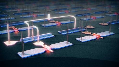 Artistic representation of the CMOS hybrid circuit used to perform the experiment: The chip contains two cells, each composed of one control transistor and one quantum device.
Inspired by dynamic random-access memory (DRAM) architecture, the hybrid electronic circuit combines conventional and quantum devices on a chip using complementary metal-oxide semiconductor (CMOS) technology, to deliver input and output signals to quantum processors while keeping the number of connections manageable, and thereby reduce the complexity of quantum computing architecture. This innovation represents another milestone in current worldwide efforts for the realization of a practical large-scale fault-tolerant quantum computer.
Quantum computers promise to solve some of the most challenging computational problems such as simulation for revolutionary new materials, chemicals and medicines. Research has demonstrated that it is now possible to build small quantum processors in a variety of hardware platforms, and their computational capabilities are approaching those of supercomputers. However, to tackle the most demanding computational simulations, it is thought that a large-scale fault-tolerant quantum computer might ultimately require 10 million quantum bits (qubits) to run the most complex of calculations(2) - a much larger number than what current technology can support.
In the quest to build that large-scale quantum computer, one important challenge is how to reduce the complexity of the quantum computing architecture. This challenge involves, for example, efficient management of the input and output (I/O) of data and the reduction of circuit elements. In current solid-state quantum processors, qubits are wired one by one, in a very similar way to how discrete components were wired in the first computers. As the number of connections increased exponentially, this posed a challenge for conventional computers which was resolved by the invention of the integrated circuit that allowed many more components with multiple functionalities to be integrated on a chip of the same size. Similarly, as quantum computers become increasingly more complex with larger numbers of qubits, the number of connections will also increase, complicating the processor architecture. Further, as quantum computers increase in size, they will eventually become incompatible with current support systems that keep the quantum chips at temperatures close to absolute zero (where quantum computers work best). To address the “I/O problem,” the team used CMOS technology to fabricate a hybrid circuit that combines digital, analogue and quantum devices all operating at ten millikelvin. The circuit which contains quantum devices interfaced by digital transistors simplifies the processor architecture as it enables efficient routing of the readout signals and reduces the number of sensors for readout. The team demonstrated that these circuits can be used to efficiently route signals to the quantum devices. Furthermore, with this circuit, the team showed how to reduce the number of sensors required for readout, by dynamically connecting the quantum devices to a single readout resonator. The concept, inspired by conventional DRAM architecture will mean an overall simplification of the quantum computer design.
Features of this work:
1. DRAM architectural concept applied to quantum signal routing
In DRAM, the memory architecture is divided into cells, each containing an information storage capacitor. Digital signals are routed to these capacitors via control transistors to enable the read and write of the information with a reduced number of inputs. In this work, the capacitor was replaced by a quantum device capable of storing single electrons – the basic computing element of a silicon-based quantum computer - and was fabricated using the same CMOS technology as the routing transistors.
2. Efficient signal routing
The team demonstrated two of these cells, controlled by a single input line and read sequentially by a single analogue sensor –a gate-based sensor(3) - specifically tailored to the quantum devices.
3. Conventional CMOS fabrication
The chips were fabricated at CEA-LETI using industrial CMOS processes. Using CMOS for quantum computing will lead to a reduction the cost of production and facilitate commercialization at scale in the future.
This research was carried out at HCL in collaboration with academic partners at the University of Cambridge, University College London and CEA-LETI, France, and was supported by funding from the European Union's Horizon 2020 research and innovation programme under grant agreement No 688539: MOS-Quito project.(4) The results have just been published in the 17 June issue of Nature Electronics.(5)
- I/O problem: J. A. Morton and W. J. Pietenpol, Proceedings of the IRE 46, 955 (1958), D.P. Franke arXiv:1806.02145v1 (2018).
- A. Fowler et al, ”Surface codes: Towards practical large-scale quantum computation,” Phys Rev A, vol 86, Issue 3, Sept. 2012.
- I. Ahmed et al, “Radio-Frequency Capacitive Gate-Based Sensing,” Phys. Rev. Applied, Vol. 10, Issue 1, July 2018.
- https://cordis.europa.eu/project/id/688539
- https://www.nature.com/articles/s41928-019-0259-5