Researchers at the Massachusetts Institute of Technology and others have invented a new class of photonic devices that allow for the accurate and scalable broadcasting of light from the chip into free space. The results were published in the journal Nature.
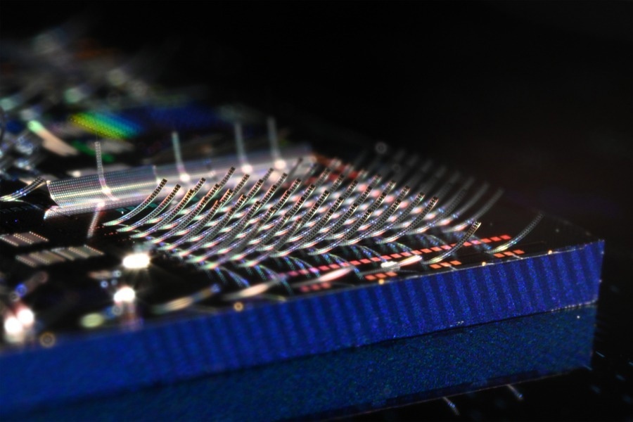 A new class of photonic chips that use light instead of electricity to process data features arrays of microscopic structures that curl upward like tiny, glowing ski jumps. Researchers can precisely control how light is emitted from thousands of these structures simultaneously. Image Credit: Massachusetts Institute of Technology
Photonic chips process data using light rather than electricity, resulting in quicker communication speeds and increased bandwidth. The majority of that light often remains on the chip, trapped in optical wires, making it difficult to communicate with the outside world efficiently.
If a significant amount of light could be beamed off the chip quickly and precisely, free of the limitations of the wiring, it might pave the way for higher-resolution displays, smaller Lidar systems, more precise 3D printers, and larger-scale quantum computers.
Their chip employs an array of small structures that spiral upward, mimicking little, glowing ski jumps. The researchers have precise control over how light is emitted from thousands of these small devices at once.
They utilized this new platform to display detailed, full-color images about half the size of a grain of table salt. When used in this way, the technology might help in the creation of lightweight augmented reality glasses or compact displays.
They also showed that photonic "ski jumps" could be utilized to precisely control quantum bits, or qubits, in a quantum computing system.
On a chip, light travels in wires, but in our normal, free-space world, light travels wherever it wants. Interfacing between these two worlds has long been a challenge. But now, with this new platform, we can create thousands of individually controllable laser beams that can interact with the world outside the chip in a single shot.
Henry Wen, Study Co-Lead Author and Visiting Research Scientist, Research Laboratory of Electronics, Massachusetts Institute of Technology
Co-lead authors Matt Saha of MITRE, Andrew S. Greenspon, a visiting scientist in RLE and MITRE, Matthew Zimmermann of MITRE, Matt Eichenfeld of the University of Arizona, senior author Dirk Englund, a professor in the MIT Department of Electrical Engineering and Computer Science and principal investigator in the Quantum Photonics and Artificial Intelligence Group and the RLE, and others from MIT, MITRE, Sandia National Laboratories, and the University of Arizona join him on the study.
A Scalable Platform
The Quantum Moonshot Program, a partnership between MIT, the University of Colorado at Boulder, the MITRE Corporation, and Sandia National Laboratories to create a revolutionary quantum computing platform utilizing the diamond-based qubits being produced in the Englund lab, gave rise to this study.
The researchers sought a mechanism to communicate with millions of qubits simultaneously since these diamond-based qubits are controlled by laser beams.
We can’t control a million laser beams, but we may need to control a million qubits. So, we needed something that can shoot laser beams into free space and scan them over a large area, kind of like firing a T-shirt gun into the crowd at a sports stadium.
Henry Wen, Study Co-Lead Author and Visiting Research Scientist, Research Laboratory of Electronics, Massachusetts Institute of Technology
Current techniques for directing and broadcasting light off a photonic device can't scale up to interact with millions of qubits since they usually only function with a few beams at a time.
To establish a scalable platform, the researchers used a novel manufacturing approach. Their technology results in photonic chips with small structures that curve upward from the chip's surface to emit laser beams into space.
They made these small "ski jumps" for light by constructing two-layer structures out of two distinct materials. Each material expands differently when it cools from the high manufacturing temperatures.
The researchers created the structures with unique patterns in each layer so that when the temperature changes, the variance in strain between the materials forces the entire structure to curve upward as it cools.
This is the same effect as an old-fashioned thermostat, which uses a coil of two metallic materials that curls and uncurls in response to the room's temperature, triggering the HVAC system.
Wen added, “Both of these materials, silicon nitride and aluminum nitride, were separate technologies. Finding a way to put them together was really the fabrication innovation that enables the ski jumps. This wouldn’t have been possible without the pioneering contributions of Matt Eichenfield and Andrew Leenheer at Sandia National Labs.”
On the chip, connected waveguides direct light to the ski jump structures. The researchers use a series of modulators to quickly and accurately regulate how the light is switched on and off, allowing them to project it off the chip and move it about in free space.
Painting with Light
They can broadcast light in a variety of colors and control the density of the pattern emitted by adjusting the light frequencies. This allows them to effectively create images in free space using light.
This system is so stable we don’t even need to correct for errors. The pattern stays perfectly still on its own. We just calculate what color lasers need to be on at a given time and then turn it on.
Henry Wen, Study Co-Lead Author and Visiting Research Scientist, Research Laboratory of Electronics, Massachusetts Institute of Technology
Since individual points of light, or pixels, are so small, researchers can use this platform to create extraordinarily high-resolution screens. For example, according to Wen, their technology allows them to pack 30,000 pixels into the same region that can only store two pixels on smartphone displays.
“Our platform is the ideal optical engine because our pixels are at the physical limit of how small a pixel can be,” he added.
Beyond high-resolution screens and bigger quantum computers utilizing diamond-based qubits, the technique might be utilized to create Lidars small enough to fit on tiny robots.
It might also be used in 3D printing, which creates objects by curing layers of resin using lasers. Since their technology creates controllable beams of light so quickly, it might significantly speed up these printing processes, allowing users to construct more complicated objects.
In the future, the researchers hope to scale up their system and do further studies on light yield and uniformity, develop a larger system to capture light from an array of photonic chips with "ski jumps," and undertake robustness tests to see how long the devices endure.
“We envision this opening the door to a new class of lab-on-chip capabilities and lithographically defined micro-opto-robotic agents,” Wen concluded.
This study was partially financed by the MITRE Quantum Moonshot Program, the US Department of Energy, and the Center for Integrated Nanotechnologies.
Sources:
Journal Reference:
Saha, M. et al. (2025) Nanophotonic waveguide chip-to-world beam scanning. Nature. DOI: 10.1038/s41586-025-10038-6. https://www.nature.com/articles/s41586-025-10038-6.
Massachusetts Institute of Technology