Feb 15 2019
Researchers from the U.S. Naval Research Laboratory (NRL) and the Air Force Research Laboratory (AFRL) have devised a technique for directly writing quantum light sources, emitting a single light photon at a time, into monolayer semiconductors like tungsten diselenide (WSe2).
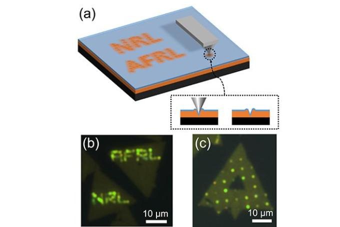 (a) Illustration showing an AFM tip indenting the TMD/polymer structure to introduce local strain. (b) Patterned single-photon emission in WSe2 induced by AFM indentation of the letters “NRL” and “AFRL.” (c) AFM indents produce single-photon emitter “ornaments” on a monolayer WSe2 “Christmas tree.”
Single-photon emitters (SPEs), or quantum emitters, are vital components in an extensive range of nascent quantum-based technologies, such as secure communications, computing, metrology, and sensing.
When compared to traditional light emitting diodes that emit billions of light photons at the same time to produce a steady stream of light, an ideal SPE produces precisely one photon on demand, where each photon cannot be differentiated from another. These properties are crucial for photon-based quantum technologies that are currently being developed. Moreover, capabilities such as these should be achieved in a material platform that enables repeatable, precise placement of SPEs in a completely scalable fashion that is consistent with prevalent semiconductor chip manufacturing.
The researchers at NRL employed an atomic force microscope (AFM) to form nanoscale indents or depressions in a single WSe2 monolayer on a polymer film substrate. A highly localized strain field generated around the nano-indent produces the SPE state in the WSe2. Time-correlated measurements of this light emission carried out at AFRL confirmed the true single-photon nature of these states. These emitters are bright, generating single photons at higher rates, and are spectrally stable, major requirements for evolving applications.
This quantum calligraphy allows deterministic placement and real time design of arbitrary patterns of SPEs for facile coupling with photonic waveguides, cavities and plasmonic structures. Our results also indicate that a nano-imprinting approach will be effective in creating large arrays or patterns of quantum emitters for wafer scale manufacturing of quantum photonic systems.
Berend Jonker, PhD, Senior Scientist and Principal Investigator, U.S. Naval Research Laboratory.
Pointing out the significance of this discovery, Dr Matthew Rosenberger, lead author of the study, stated that “In addition to enabling versatile placement of SPEs, these results present a general methodology for imparting strain into two dimensional (2D) materials with nanometer-scale precision, providing an invaluable tool for further investigations and future applications of strain engineering of 2D devices.”
The outcomes of this study open the door for using 2D materials as solid-state hosts for SPEs in applications that are relevant to the mission of the Department of Defense (DoD), for example, sensing, secure communications, and quantum computation. Applications such as these allow communication between distant DoD forces that is not affected by decryption or eavesdropping, a vital requirement to guarantee the safety of the warfighter.
Quantum computation on a chip offers onboard potential for the rapid analysis of huge data sets obtained by sensor arrays, so that the need to transmit the entire data set is eliminated, thus minimizing bandwidth requirements. The results of the study have been published in ACS Nano in January 2019.
The research team included Dr Matthew Rosenberger, Dr Hsun-Jen Chuang, Dr Saujan Sivaram, Dr Kathleen McCreary, and Dr Berend Jonker from the NRL Materials Science and Technology Division; and Dr Chandriker Kavir Dass and Dr Joshua R. Hendrickson from the AFRL Sensors Directorate. Both Rosenberger and Sivaram hold National Research Council (NRC) fellowships at NRL, and Chuang holds an American Society for Engineering Education (ASEE) fellowship at NRL.