Researchers at the University of California, Riverside, discovered how to control electrical flow through crystalline silicon, a material at the core of modern technology. The discovery could lead to smaller, quicker, and more efficient electronics by leveraging quantum electron behavior. The study was published in the Journal of the American Chemical Society.
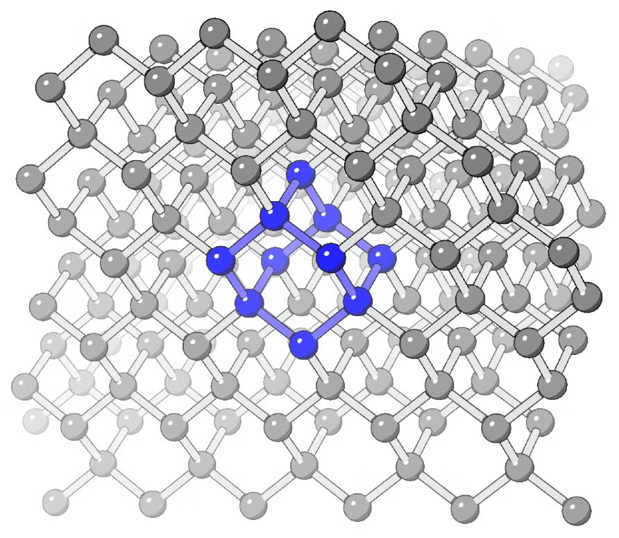
Crystalline silicon. Chemical structure of bulk silicon, with the simplest building block of the solid highlighted in blue. Image Credit: Tim Su/UCR
On the quantum scale, electrons act more like waves than particles. Scientists have recently demonstrated that the symmetrical structure of silicon molecules can be fine-tuned to induce or suppress a phenomenon called destructive interference. The effect can toggle conductivity “on” or “off,” acting as a molecular-scale switch.
We found that when tiny silicon structures are shaped with high symmetry, they can cancel out electron flow like noise-canceling headphones. What’s exciting is that we can control it.
Tim Su, Study Lead and Professor, University of California, Riverside
The study advances the understanding of how electricity travels through silicon at the atomic level.
The finding comes as the tech sector struggles to reduce the size of traditional silicon chips. Traditional approaches include cutting tiny circuits into silicon wafers or doping, which involves adding small amounts of other elements to modify how silicon conducts electricity.
Although these methods have been effective for decades, they're now approaching their physical limits: there’s a limit to how small things can be carved, and adding more atoms doesn't address the challenges introduced by quantum effects.
In contrast, Su and his team employed chemistry to construct silicon molecules from the ground up, rather than cutting them down. This “bottom-up” method allowed them to precisely regulate how the atoms were placed and, more importantly, how electrons moved through their silicon devices.
Silicon is the second most abundant element in the Earth’s crust and the primary component of computing. However, when devices shrink, unanticipated quantum effects, such as electrons leaking through insulating barriers, make classic designs more difficult to govern. This new study argues that engineers should embrace, rather than oppose, quantum behavior.
Su added, “Our work shows how molecular symmetry in silicon leads to interference effects that control how electrons move through it. And we can switch that interference on or off by controlling how electrodes align with our molecule.”
While the concept of exploiting quantum interference in electronics is not novel, this is one of the first examples of the phenomenon in three-dimensional, diamond-like silicon, the same structure utilized in commercial chips.
Beyond ultra-small switches, the findings could help develop thermoelectric devices that turn waste heat into electricity, as well as quantum computing components made of familiar materials.
“This gives us a fundamentally new way to think about switching and charge transport. It’s not just a tweak. It’s a rethink of what silicon can do,” added Su.
Journal Reference:
Hight, M. O., et al. (2025) Quantum Interference in a Molecular Analog of the Crystalline Silicon Unit Cell. Journal of the American Chemical Society. doi.org/10.1021/jacs.5c04272.