"The interface is the device," Nobel laureate Herbert Kroemer famously observed, referring to the remarkable properties to be found at the junctures where layers of different materials meet. In today's burgeoning world of nanotechnology, the interfaces between layers of metal oxides are becoming increasingly prominent, with applications in such high-tech favorites as spintronics, high-temperature superconductors, ferroelectrics and multiferroics.
Realizing the vast potential of these metal oxide interfaces, especially those buried in subsurface layers, will require detailed knowledge of their electronic structure. A new technique from an international team of researchers working at Berkeley Lab's Advanced Light Source (ALS) promises to deliver the goods.
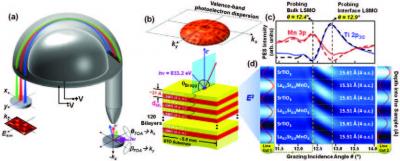 This image shoes the experimental setup and basic principles of SWARPES including (a) the experimental setup; (b) diagram of the multilayer STO and LSMO film; (c) SW-excited photoemission intensity rocking curves and (d) simulated intensity of the x-ray standing wave field as a function of the depth and grazing incidence angle. Credit: Photo courtesy of Charles Fadley, UC Davis/Berkeley Lab
In a study led by Charles Fadley, a physicist who holds joint appointments with Berkeley Lab's Materials Sciences Division and the University of California Davis, where he is a Distinguished Professor of Physics, the team combined two well-established techniques for studying electronic structure in crystalline materials into a new technique that is optimized for examining electronic properties at subsurface interfaces. They call this new technique SWARPES, for Standing Wave Angle-Resolved Photoemission Spectroscopy.
"SWARPES allows us for the first time to selectively study buried interfaces with either soft or hard x-rays," Fadley says. "The technique can be applied to any multilayer prototype device structure in spintronics, strongly correlated/high-TC superconductors, or semiconductor electronics. The only limitations are that the sample has to have a high degree of crystalline order, and has to be grown on a nanoscale multilayer mirror suitable for generating an x-ray standing wave."
As the name indicates, SWARPES combines the use of standing waves of x-rays with ARPES, the technique of choice for studying electronic structure. A standing wave is a vibrational pattern created when two waves of identical wavelength interfere with one another: one is the incident x-ray and the other is the x-ray reflected by a mirror. Interactions between standing waves and core-level electrons reveal much about the properties of each atomic species in a sample. ARPES from the outer valence levels is the long-standing spectroscopic workhorse for the study of electronic structure. X-rays striking a material surface or interface cause the photoemission of electrons at angles and kinetic energies that can be measured to obtain detailed electronic energy levels of the sample. While an extremely powerful tool, ARPES, a soft x-ray technique, is primarily limited to the study of near-surface atoms. It's harder x-ray cousin, HARPES, makes use of more energetic x-rays to effectively probe subsurface interfaces, but the addition of the standing wave capability provides a much desired depth selectivity.
"The standing wave can be moved up and down in a sample simply by rocking the angle of incidence around the Bragg angle of the mirror," says Alexander Gray, a former member of Fadley's UC Davis research group and affiliate with Berkeley Lab's Materials Sciences Division, who is now a postdoctoral associate at Stanford/SLAC. "Observing an interface between a ferromagnetic conductor (lanthanum strontium manganite) and an insulator (strontium titanate), which constitute a magnetic tunnel junction used in spintronic logic circuits, we've shown that changes in the electronic structure can be reliably measured, and that these changes are semi-quantitatively predicted by theory at several levels. Our results point to a much wider use of SWARPES in the future for studying the electronic properties of buried interfaces of many different kinds."