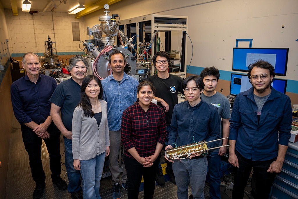
Members of the team that conducted the research. Theory lead Liang Tan is holding one of the ion accelerators used to form quantum light emitters in silicon. (Left to right: Thomas Schenkel, Takeshi Katayanagi, Qing Ji, Arun Persaud, Kaushalya Jhuria, Wei Liu, Liang Tan, Yertay Zhiyenbayev, and Walid Redjem). Image Credit: Thor Swift/Berkeley Lab
The successful transport of quantum information means working with individual photons rather than the light sources used in conventional fiber optic networks. Scientists are thus turning to quantum light emitters, also known as color centers, to produce and manipulate individual photons.
In semiconductor materials, these atomic-scale defects can emit single photons of fixed wavelength or color and allow photons to interact with electron spin properties in a controlled manner.
In this light, a research group has recently illustrated a highly effective method for making quantum emitters utilizing pulsed ion beams, thereby increasing the current understanding of how quantum emitters are formed.
The study was headed by Department of Energy Lawrence Berkeley National Laboratory (Berkeley Lab) researchers Thomas Schenkel, Liang Tan, and Boubacar Kanté, an associate professor of electrical engineering and computer sciences at the University of California, Berkeley.
The results of the study were published in the journal Physics Review Applied and are part of a larger effort by the group to determine the best quantum defect emitters for processing and transporting quantum information and to produce them with accuracy.
The color centers we’re making are candidates for becoming the backbone of a quantum internet and a key resource for scalable quantum information processing. They could support linking quantum-computing nodes for scalable quantum computing.
Thomas Schenkel, Study Senior Scientist in Berkeley Lab’s Accelerator Technology, Applied Physics (ATAP) Division, University of California, Berkeley
As part of their efforts, the team focused on the fabrication of a specific type of color center in silicon, comprising two substitutional carbon atoms and a slightly dislodged silicon atom.
The more traditional way to produce the defects is to hit the silicon with a continuous beam of high-energy ions; however, the researchers identified that a pulsed ion beam is significantly more efficient, producing many more of the desired color centers.
“We were surprised to find these defects can be more easily generated with pulsed ion beams. Right now, industry and academia mainly use continuous beams, but we’ve demonstrated a more efficient approach,” stated Wei Liu, a postdoctoral scholar in ATAP and first author of the publication.
The scientists think that the transient excitations made by the pulsed beam, where the temperature and system energetics vary quickly, are main to the highly efficient color center formation, which they fixed via an earlier study utilizing pulsed ion beams from a laser-driven accelerator reported in the journal Communications Materials.
The team characterized the color centers at cryogenic temperatures using highly sensitive near-infrared detectors to probe their optical signals.
They soon discovered that the intensity of the ion beam used to create the color centers altered the optical properties of the photons emitted.
Large-scale computer simulations on the Perlmutter system at the National Energy Research Scientific Computing Center (NERSC) provided further insight into the discovery, revealing that the wavelength of emitted photons is sensitive to strain in the crystal lattice.
“First-principles electronic structure calculations have become the go-to method for understanding defect properties. We have reached the point where we can predict how a defect behaves, even in complex environments,” added Vsevolod Ivanov, a postdoctoral scholar at the Molecular Foundry and co-first author of the publication.
The team's findings also suggest a novel application for quantum emitter color centers as sensors for radiation.
It opens new directions. We can form this color center by just hitting silicon with a proton. We could potentially use that as a dark-matter or neutrino detector with directionality because we see these different strain fields depending on which way the radiation came.
Liang Tan, Staff Scientist, Berkeley Lab’s Molecular Foundry, University of California, Berkeley
With this deeper knowledge of quantum emitter formation and properties, the group hopes to continue exploring color centers.
Future work will include the creation of a database of color centers predicted to exist in silicon, using computer simulations to identify those best suited to quantum computing and networking applications, and refining fabrication techniques to gain deterministic control over creating individual color centers.
We’re working towards a new paradigm of qubits by design. Can we reliably make a given color center that operates in the telecom band, has sufficient brightness, isn’t too hard to make, has a memory, etcetera? We’re engaged in that quest and have demonstrated some exciting progress.
Boubacar Kanté, Associate Professor of Electrical Engineering and Computer Sciences, University of California, Berkeley
“The new pathways to forming color centers using intense beams uncovered in this work are an exciting application of high energy density conditions and plasma science to improving technologies for quantum information science,” stated ATAP Division Director Cameron Geddes.
The Molecular Foundry and National Energy Research Scientific Computing Center (NERSC) are DOE Office of Science user facilities situated at Berkeley Lab.
This study was financially supported by the DOE Office of Science’s Fusion Energy Sciences and High Energy Physics programs.
Journal Reference:
Liu, W., et al. (2023) Quantum Emitter Formation Dynamics and Probing of Radiation-Induced Atomic Disorder in Silicon. Physical Review Applied. doi.org/10.1103/PhysRevApplied.20.014058.