Image Credit: dominika zara/Shutterstock.com
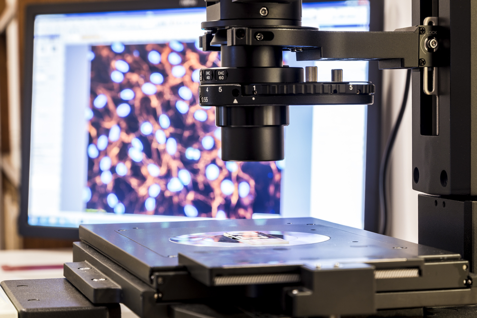
Scanning probe microscopy (SPM) techniques are a class of imaging techniques that rely on the interaction between an atomically sharp tip and a surface to identify and characterize the topology of the sample. The two main methods that fall within this class are scanning tunneling microscopy (STM) and atomic force microscopy (AFM). However, many other variations have core operational principles that are centered around these techniques.
Introduction
SPM techniques are primarily concerned with imaging a surface of a larger material at the nanoscale. Because SPM techniques image at the minute scale, quantum effects come in to play as a result of the properties of the nanomaterial that are typically governed by quantum effects rather than bulk classical effects.
To interact with and image the nanoscale surface, quantum mechanical effects arise from the SPM instruments to allow for their interaction on the same energy level as that which is present on the sample’s surface. These quantum effects also govern how SPM functions from an operational perspective, in addition to relying on quantum tunneling to perform measurements. Several other phenomena are involved with SPM instruments, such as piezoelectric interactions; however, such effects are not quantum mechanical.
Electron Tunneling
Electron tunneling is a quantum mechanical phenomenon that is based around the particle in a box theory, otherwise known as a particle in a well theory. The particle in a box theory states that if an electron is confined to an imaginary box with defined boundaries in either 1, 2, or 3 dimensions, which depends on whether the ‘box’ is 1D, 2D or 3D, then the electron physically cannot escape these boundaries.
The only way in which the electron can interact with other electrons and/or atoms outside of the box is to ‘tunnel’ its way out. Tunneling is essentially the extension of the electron’s wavefunction beyond the ‘box,’ which can then enable the electron to interact with other species.
This may seem a strange concept at first glance because the electron is a particle. However, much like photons, at the quantum level, electrons have wavelike properties. This means that their reach is further than that which is present in classical bulk systems.
This reach can extend beyond the ‘barrier’ of the box (or in more practical scenarios, the potential/quantum well that it is confined within) into other regions.
In many nanotechnology applications, the wavefunction of the electron extends into other potential wells where other electrons are located, enabling the electrons to interact with each other. When the electron can move in this fashion, the overall process is known as tunneling, with quantum tunneling and electron tunneling often being used interchangeably.
This effect is the quantum mechanical basis for SPM imaging methods, as well as for governing the electronic interaction between quantumly confined nanomaterials like quantum dots, nanowires and 2D materials.
Tunneling Applied to SPM
Electron tunneling is a phenomenon that is not unique to SPM. However, its principles can be applied in a specific way to the imaging of a sample’s surface. For SPM, it is the interaction between the apex atom on the atomically sharp tip and the atoms present on the surface of the material under analysis that facilitates the electron tunneling process.
Because the surface of the sample often contains many atoms, each individual particle behaves as an individual potential well. The tip has a single atom at its finest point of the tip, and as it scans across the surface of the material, a voltage bias is applied.
Between the potential well of the tip and the atom lies an electronic gap, otherwise known as a potential barrier. If the two potential wells of the tip and the surface are close enough to each other, the electron will move from the side of the tip, across the potential barrier, and into the potential well of the surface. If the bias is continually applied, the electrons will continue to move across the potential barrier generating a ‘tunneling current’. This current is used to map the surface as the instrument and the sample are electronically connected.
In STM, the tip is kept at a fixed point away from the sample to maintain this current, and any changes in height or position can be recorded as a result. While the tunneling current is maintained across the surface, scanners are used to measure the relative position of the atoms, while a feedback loop monitors and maintains the current.
In AFM, the voltage bias enables electrons to tunnel between the top and the surface. However, the specific interactions that cause the tip to move towards the surface are based around interatomic interactions. In conclusion, the working mechanism of AFM is slightly different as compared to other SPM methods.
References and Further Reading
- “Scanning probe microscopes” –Aberystwyth University
- “Scanning Tunnelling Microscopy” –nanoScience Instruments
- “Chapter 6 Theory of Scanning Tunnelling Microscopy”- Louis S., 45th IFF Spring School: Computing Solids: Models, Ab-initio Methods and Supercomputing organized at the research center of Juelich, 2014.
Disclaimer: The views expressed here are those of the author expressed in their private capacity and do not necessarily represent the views of AZoM.com Limited T/A AZoNetwork the owner and operator of this website. This disclaimer forms part of the Terms and conditions of use of this website.