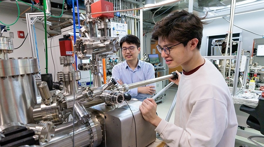
Researchers at the University of Chicago Pritzker School of Molecular Engineering, including Assistant Professor Shuolong Yang and graduate student Khanh Duy Nguyen, have identified one of the world’s thinnest naturally occurring semiconductor junctions within a promising quantum material. The study was published in the journal Nanoscale.

Researchers at the University of Chicago Pritzker School of Molecular Engineering, including Asst. Prof. Shuolong Yang (left) and graduate student Khanh Duy Nguyen, have discovered one of the world’s thinnest semiconductor junctions naturally forming within a promising quantum material. Image Credit: John Zich.
Scientists investigating a promising quantum material have made an unexpected discovery: its crystal structure naturally forms one of the thinnest known semiconductor junctions, just 3.3 nm thick, or roughly 25,000 times thinner than a sheet of paper.
This was a big surprise. We weren’t trying to make this junction, but the material made one on its own, and it’s one of the thinnest we’ve ever seen.
Shuolong Yang, Assistant Professor, University of Chicago Pritzker School of Molecular Engineering
This breakthrough not only opens the door to creating ultra-miniaturized electronic components but also sheds light on electron behavior in materials engineered for quantum technologies.
Uneven Electrons
Researchers at the University of Chicago Pritzker School of Molecular Engineering (UChicago PME) and Pennsylvania State University were exploring the electronic behavior of MnBi₆Te₁₀, a topological material known for its remarkable ability to conduct electricity along its edges without resistance. This class of materials holds promise for future quantum computers and ultra-efficient electronic devices.
To function as intended, materials like MnBi₆Te₁₀ require a precise balance and distribution of electrons. The research team aimed to achieve this by adjusting the material’s chemical composition, and introducing antimony into the structure. Standard electrical measurements indicated that the modified material was electrically neutral overall.
Then, Yang’s team took a closer look using time- and angle-resolved photoemission spectroscopy (trARPES), a technique that employs ultrafast laser pulses to observe how electrons are distributed and how their energy levels change in real-time.
What they found was surprising: within each repeating layer of the crystal (only a few atoms thick) the electrons were unevenly distributed. They clustered in certain regions, leaving others electron-deficient. This generated tiny built-in electric fields within the material.
In an ideal quantum material, you want a really uniform distribution of charges. Seeing this uneven distribution suggests that we may not enable quantum applications in the originally planned fashion, but reveals this other really useful phenomenon.
Khanh Duy Nguyen, Study First Author and Graduate Student, University of Chicago Pritzker School of Molecular Engineering
These tiny regions functioned like p-n junctions—semiconductor interfaces with internal electric fields commonly used to create diodes in everyday electronics such as phones and computers. However, unlike conventional p-n junctions that are engineered during fabrication, these formed naturally within the crystal structure itself.
A Boon for Quantum and Electronic Applications
As this newly discovered, naturally forming p-n junction is also highly sensitive to light, it holds potential for next-generation electronics, including spintronics, a technology that leverages an electron’s magnetic spin, rather than its charge, to store and process data.
Through detailed modeling of MnBi₆Te₁₀’s crystal structure, Nguyen, Yang, and their colleagues developed a hypothesis about how these junctions form. They propose that introducing antimony into the material triggers atomic swapping between manganese and antimony atoms, creating a charge imbalance.
While the discovery adds complexity to using MnBi₆Te₁₀ for certain quantum effects, it also unlocks new possibilities for electronic applications. It paves the way for further engineering of the material to achieve a more uniform electron distribution, enhancing its potential for use in quantum technologies.
The UChicago PME team is now refining methods to fabricate thin films of MnBi₆Te₁₀, rather than bulk 3D crystals. This approach could offer greater control over electron behavior, either to enhance desired quantum properties or to increase the formation of naturally occurring p-n junctions.
This once again demonstrates the value of pursuing basic, fundamental scientific research and being open about where it leads. We set out with one goal and found a surprise that led us in another, really exciting direction.
Shuolong Yang, Assistant Professor, University of Chicago Pritzker School of Molecular Engineering
This research was supported by the US Department of Energy (DE-SC0022960) and the National Science Foundation through the Penn State 2D Crystal Consortium–Materials Innovation Platform (2DCC-MIP) under NSF Cooperative Agreement DMR 2039351.
Journal Reference:
Nguyen, K. D., et al. (2025) Spectroscopic evidence of intra-unit-cell charge redistribution in a charge-neutral magnetic topological insulator. Nanoscale. doi.org/10.1039/d4nr04812a.