In our latest interview, Assistant Professor Shuolong Yang from the Pritzker School of Molecular Engineering discusses a new topological superconductor to carry quantum information, and how its production method was inspired by paper block printing.
Could you introduce yourself and your background in materials science and quantum technology?
I am an assistant professor at the University of Chicago’s Pritzker School of Molecular Engineering. I am a materials scientist and solid-state physicist who specializes in the fabrication and characterization of novel quantum materials and structures. In particular, my laboratory has been producing atomically thin materials for future quantum technologies, including topological quantum computing.
What are quantum computers and how do they differ from conventional computers?
Quantum computers utilize a new kind of information carrier – quantum bits (qubits), as compared to the classical bits in classical computers. Classical bits have two deterministic states: zero and one. A qubit can be in a superposition state, which represents zeros and ones simultaneously. This is how a qubit can in principle carry exponentially more information than a classical bit. It is estimated that to describe the position of all atoms in the universe, one only needs 616 qubits. Quantum computers can in principle help us solve problems that could never be done by classical computers, such as the behaviors of complex materials and predictions of new drugs.
What issues are holding quantum computers back from full realization?
One issue is how to incorporate more qubits while maintaining quantum coherence. It turns out that qubits using current implementations, such as traditional superconductors, are rather vulnerable. Errors can easily destroy the “quantumness” of the qubits, which leads to the loss of quantum information. Another issue is that many quantum computers can only work at exceedingly low temperatures (milli-Kevin range, or a few thousandths of Fahrenheit above absolute zero).
What are topological materials and why are they useful for this application?
Topological materials are materials where the electronic properties are protected by their innate symmetries, and not easily disturbed by impurities and defects. Topology is rather a mathematical concept. Physicists borrow it due to a formal mathematical analogy. Imagine that we have a donut with a hole in the middle. If we do not change the topology of this donut but continuously deform it, i.e., we do not fill the middle hole or break the ring, we will never make the middle hole disappear even though the shape can be different. Physicists use this concept to describe the electronic properties of topological materials. It turns out that they carry some unique surface or edge currents, which act exactly like the middle hole of the donut. If we throw some general impurities on the materials or introduce certain types of electromagnetic radiation on them, these surface or edge currents will be undisturbed. As a matter of fact, they may provide a potential solution to circumvent the first issue mentioned above – the quantum error problem.
What are some of the challenges with using these materials, and how did you tackle them?
The current challenges for using these materials are that we still have not found the perfect material candidates which can exhibit the desired topological properties at realistic temperatures and macroscopic scales. Moreover, even though materials scientists have identified a few promising candidates, it is generally difficult to make devices out of these materials, as many of them are unstable in atmosphere. This also makes the characterization of these materials extremely difficult.
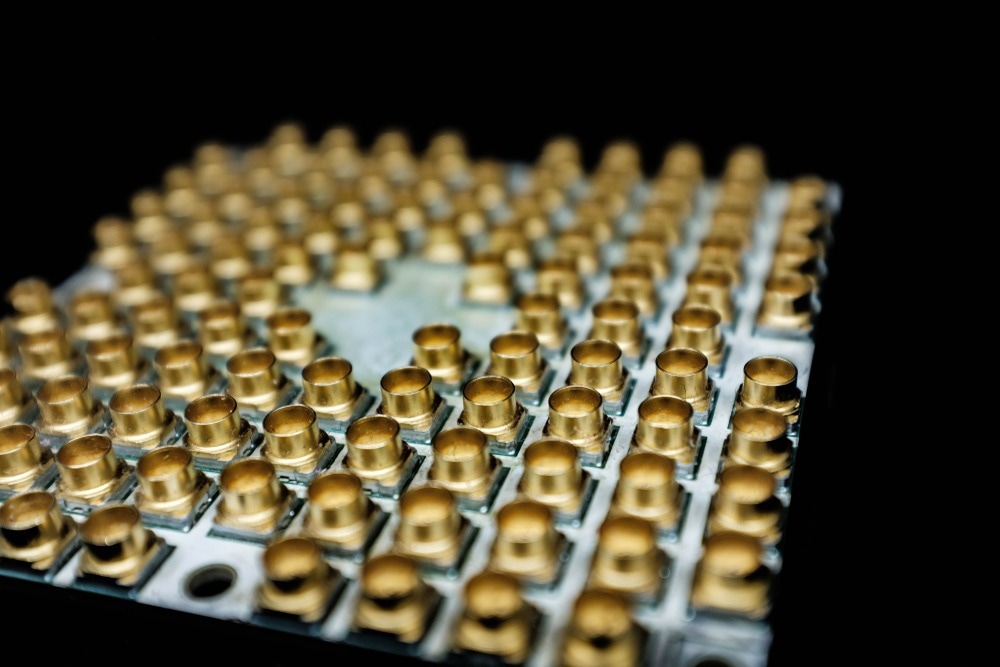
Image Credit: Craig Raymond/Shutterstock.com
In my laboratory, we directly connect an advanced material deposition tool – molecular beam epitaxy, with a material characterization tool – angle-resolved photoemission spectroscopy. The two setups operate in an ultrahigh vacuum environment, which is comparable to outer space. Moreover, these two vacuum systems are directly connected – this is like an inverse space station. Compared to a real space station, here we keep air outside and vacuum inside. This way we produce promising materials with layer-by-layer control and characterize their topological electronic properties while they are still pristine in an ultrahigh vacuum.
My Quantum Manufacturing proposal is to tackle the challenge of making meaningful quantum devices out of promising topological materials. The idea is not to follow the traditional nanofabrication protocol, in which materials will need to be taken to the atmosphere and undergo a tedious process using chemical etching and electron-beam bombardment. Here, we will print the devices directly during the deposition stage. The main idea is to pre-pattern the substrates, such that the thin films can only grow in selected areas.
You have proposed the use of a new topological superconductor to carry quantum information. Could you please describe this material and why it is significant?
This material is ultrathin FeTexSe1-x grown on SrTiO3 substrates. Here the x subscript means that the Te:Se ratio can be varied, and we are still investigating what the correct range for x is. This material is significant, as it is one of the few intrinsic topological superconductors that combine nontrivial topological properties with superconductivity. This means that we may potentially build a quantum computer using these superconductors, but at the same time, the qubits are protected from errors. If this can be done, it will be really exciting news to the quantum community. Moreover, there is high hope for the FeTexSe1-x thin films to be working at relatively high temperatures, up to the liquid nitrogen boiling point of 77 Kelvin (or -321 Fahrenheit).
The manufacturing process for this material is inspired by block printing. What led you to this source of inspiration?
In order to test the topological protection on the FeTexSe1-x thin films, we need to pattern the film into a particular device – so-called Josephson junctions. Traditionally scientists and engineers would have to use nanofabrication in a clean room, which involves a very tedious process of chemical etching and electron-beam bombardment. The material is unfortunately not stable in air, let alone the harsh chemical environment in nanofabrication. Therefore, we aim to find a new way to draw patterns on these quantum materials.
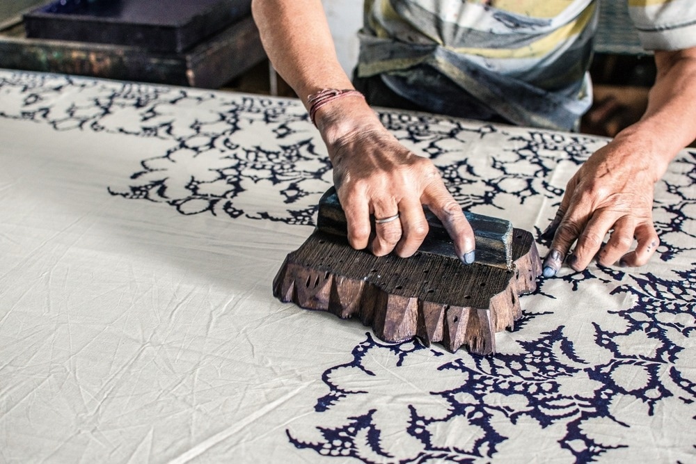
Image Credit: Alexandra Morrall/Shutterstock.com
We are inspired by block printing, as it is a way to draw patterns without having to pattern the paper itself. Instead, ancient people would first draw patterns on a woodblock, and cover it with ink. By pressing a piece of paper on the block, a pattern is drawn on the paper. We were inspired by this process and thought that we could pre-pattern the substrate, and use the substrate as the “block” for block printing quantum devices. This process happens during the deposition stage, and hence the material will never have to leave the pristine ultrahigh vacuum environment.
How does your printing process work?
An oxide substrate will first be pre-patterned, leaving plateaus at nanoscales to define the selected areas of growth. The substrate is rather inert in air, and hence all the nanofabrication steps can be done comfortably. The substrate will serve as a nanoscale “block.” We transfer the substrate into the molecular beam epitaxy system and directly grow FeTexSe1-x thin films onto the substrate. Because the substrate is pre-patterned, the films will only grow on the pre-defined areas, and hence a device will be made. Before taking the device out for testing, we will further coat the material with a protection layer.
What is a Josephson junction and how can your process be used to make one?
A Josephson junction is a superconductor-insulator-superconductor junction. It is the fundamental unit of a superconducting qubit, and hence a fundamental component of a quantum computer. The “block printing” process will potentially enable the fabrication of Josephson junctions since the superconductor will be deposited only at selected regions. This makes the manufacturing of superconductor-insulator-superconductor devices a straightforward process.
What is the difference between Majorana fermion-created qubits and “traditional” qubits, and how could your research lead to proof of their existence?
The Majorana fermion-created qubits utilize the so-called Majorana zero modes for carrying the quantum information. These are fundamentally new objects in condensed matter physics, which, to put it in a simple way, is a superposition state of traditional superconducting charge carriers that exist at multiple energy levels. They obey fundamentally new laws of physics, and in general immune to classical and quantum errors. To prove their existence, we will create a Josephson junction, where a superconducting current is tunneled through the insulating gap between two superconductors. If the Majorana zero modes exist, we will see the superconducting current oscillate at a distinct frequency.
What was personally the most exciting or memorable part of this research for you?
I am an experimentalist, so I will be honest and say that the most memorable part of this project so far was the moment when we actually created this material. We even observed the spectroscopic evidence for the existence of a key electronic state – the topological surface state. These experimental progresses enabled us to conceive the idea of “block printing.”
What is next for this research? What needs to be done before it can be implemented?
The immediate next step is to fully optimize the FeTexSe1-x material growth, and understand what chemical composition, thickness, and other conditions can lead to the desired topological properties. After that, we will attempt the proposed block printing. It will be a systematic effort involving printing, testing, re-printing, and re-testing. This idea is very disruptive, and many details need to be figured out. On the other hand, this is exactly what makes it exciting for scientists!
More from AZoQuantum: A New Algorithm Allows Quantum Computers to Perform Faster Prime Factorization
Where can readers find more information?
Here is the press release article from the Pritzker School of Molecular Engineering.
https://pme.uchicago.edu/news/uchicago-researcher-awarded-nsf-grant-manufacture-advanced-quantum-materials
Here is the NSF grant page: https://www.nsf.gov/awardsearch/showAward?AWD_ID=2240489&HistoricalAwards=false
About Shuolong Yang
I am a junior faculty member at UChicago’s Pritzker School of Molecular Engineering. My overall career mission is to create new quantum materials and structures which can enable new modes of information processing – topological electronics and topological quantum computing. To push towards this direction, I integrate creative layer-by-layer material synthesis with layer-by-layer spectroscopic characterization. So far, my group has built the first platform connecting molecular beam epitaxy with a multi-resolution photoemission spectroscopy setup. This enables us to grow and characterize materials in time, space, energy, and momentum. My effort has been recognized by the Kavli postdoctoral fellowship from Cornell, NSF CAREER award, and the DoE Early Career award.
Interview Questions Supported by Robert Lea
Disclaimer: The views expressed here are those of the interviewee and do not necessarily represent the views of AZoM.com Limited (T/A) AZoNetwork, the owner and operator of this website. This disclaimer forms part of the Terms and Conditions of use of this website.