The HDAWG multi-channel Arbitrary Waveform Generator from Zurich Instruments has been developed for sophisticated signal generation of up to 750 MHz bandwidth. It has the highest channel density among its range.
The HDAWG multi-channel Arbitrary Waveform Generator comes with four or eight single-ended, DC-coupled analog output channels with a vertical resolution of 16 bits.
An amplified mode and a direct mode with excellent noise performance and the highest maximized bandwidth support output switching. This amplified mode also increases the signal amplitude to as high as 5 Vpp. With two markers provided for each channel, accurate setup synchronization is ensured, while the full 16-bit output resolution is also maintained.
HDAWG High-Density Arbitrary Waveform Generator
Video Credit: Zurich Instruments
LabOne® offers an advanced programming concept that integrates the flexibility and performance of a random waveform generator along with the accessibility of a function generator.
Thanks to the LabOne® user interface as well as a range of APIs for C, Python, .NET, LabVIEW™, and MATLAB®, automatic measurement and rapid integration into a prevalent control setting can be achieved.
Key Features
- Maximum channel density
- Can be scaled up to 144 output channels
- Maximum signal amplitude of 5 Vpp
- 16 bits, 2.4 GSa/second, 750 MHz signal bandwidth
- LabOne® AWG Sequencer and Compiler
- Digital modulation at numerous frequencies
- Trigger-to-output delay is less than 50 ns
Applications
- Semiconductor testing
- EPR and NMR spectroscopy
- Lidar and radar
- Quantum computing
- MIMO methods in telecommunication and MRI
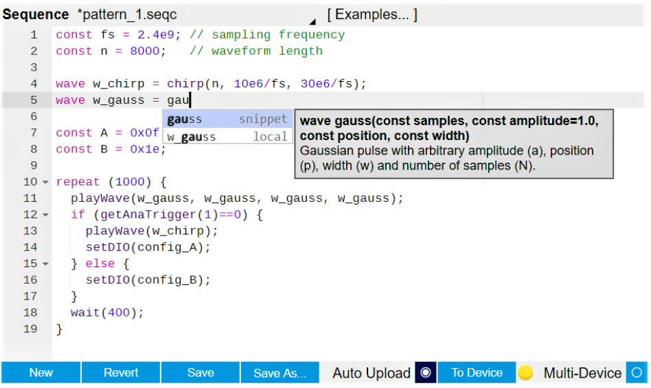
High-Level AWG Programming
The sequences and waveforms are defined in the LabOne® AWG Sequencer. Once this process is completed, the LabOne® AWG Compiler takes over, decoding the instructions into machine language and transferring the outcome to the hardware in minimal time. Loops with dynamically differing delay as well as conditional branching points are supported by the LabOne® sequencing.
Apart from the standard waveforms (like sinc, Blackman, Gaussian, and so on), the LabOne® includes all the important math and array editing tools needed for an intricate waveform design.
Users can also cut, multiply, add, and concatenate the waveforms to arrange them in segments. With a simple drag-and-drop action, quantified signals or waveforms computed with MATLAB®, for example, can be imported.
Multi-Device Synchronization
Multi-Device Synchronization (MDS) allows numerous HDAWGs to be operated as one multi-channel AWG:
- All output channels can be fully synchronized
- All instruments can be operated from a single API or LabOne user interface
- Synchronization of time stamps and sampling rates of all HDAWGs
- Phase locking of all instrument clocks
If numerous instruments are utilized, the LabOne® AWG Compiler handles the distribution of the master sequence program over all instruments. Synchronized playback timing is ensured by an automated trigger exchange procedure.
Oscillators, Modulation and Phase Control
The HDAWG multi-channel Arbitrary Waveform Generator is fitted with digital oscillators to produce the sinusoidal carrier of a signal without depending on the programmed AWG envelope signal. This implies that users can produce long signals with very rapid waveform upload and accurate phase coherence over several pulses. Moreover, users can freely modify and sweep the carrier frequencies and phases that would otherwise be written to a static waveform.
The number of oscillators is increased through the HDAWG-MF Multi-Frequency option, enabling complete digital I/Q modulation for phase cycling, frequency multiplexing, and phase and frequency modulation.
Low-Latency Triggering and Sequence Branching
Due to the low-latency design, the HDAWG multi-channel Arbitrary Waveform Generator can produce its first sample on the signal output within 50 ns after it identifies an external trigger on one of the trigger inputs provided on the front panel.
This is crucial for feedback experiments in quantum computing in which the device has short-lived properties, and every nanosecond that is saved dramatically enhances the experimental result. The instrument’s four or eight output channels can be assembled into units of two or four. Each group can be subsequently triggered separately, which boosts flexibility when distributing signals to isolate the components of a setup.
To create signals with real-time control and high complexity, the HDAWG multi-channel Arbitrary Waveform Generator is capable of choosing from a total of 1024 pre-stored waveforms in a programmable memory depending on the bit-pattern applied to its 32-bit digital input. These might represent a multi-qubit state readout result, a device-specific test waveform, or a digital modulation pattern.
Functional Description
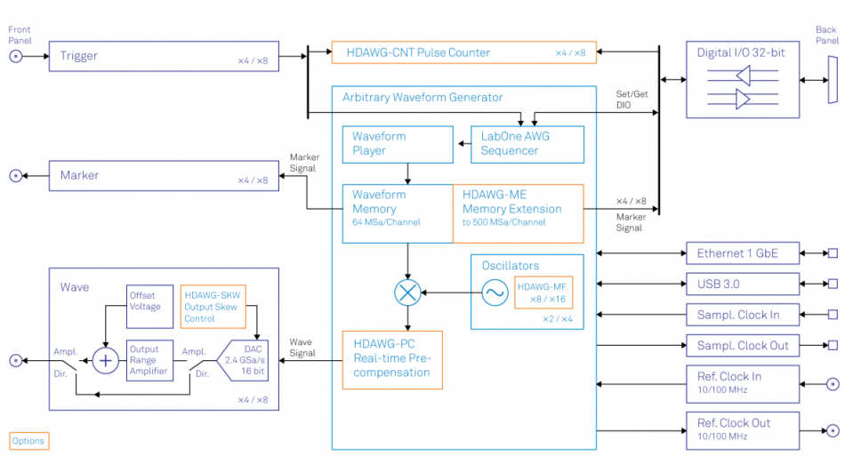
Image Credit: Zurich Instruments
HDAWG Specifications
Source: Zurich Instruments
| Arbitrary waveform generator |
| Channels |
4 (HDAWG4 model)
8 (HDAWG8 model) |
| Vertical resolution |
16 bits |
| Waveform memory per channel |
64 MSa;
500 MSa (with HDAWG-ME option) |
| Sequence length |
8,192 |
| Waveform granularity |
16 samples |
| Minimum waveform length |
32 samples |
| Sequencer clock frequency |
Sampling rate divided by 8 |
| Sequencer instructions (playback) |
Play waveform (single or multi-channel),
play waveform segment (start sample index and segment length),
play waveform from the library (DIO input state), interrupt waveform playback |
| Sequencer instructions (other) |
Wait constant, wait for trigger, set/get trigger state, set/get DIO state,
integer variable operations (add, subtract, logical operations),
change oscillator frequency/phase (real-time), change other instrument setting (non real-time) |
| Sequencer control structures |
Repeat (1 to 223-1 or infinite), conditional branch (multi-branch) |
| Wave Signal Output |
| Connector type |
SMA (front panel, single-ended) |
| Output impedance |
50 Ω |
| Output coupling |
DC |
| Output modes |
Amplified, direct |
| Output range |
±0.1 V to ±2.5 V (amplified, into 50 Ω)
±0.4 V (direct) |
| Output level accuracy |
±(1% of setting + 5 mVpp) (amplified, into 50 Ω) |
| Output level resolution |
< 0.1 mV |
| Offset voltage |
0.5 × peak voltage, max. ±1.25 V (amplified, into 50 Ω)
0 V (direct) |
| Offset voltage accuracy |
±(1% of setting + 5 mV) |
| Phase noise |
< -135 dBc/Hz (amplified, 1 Vpp, 100 MHz, offset 10 kHz)
< -148 dBc/Hz (amplified, 1 Vpp, 100 MHz, offset 1 MHz)
< -135 dBc/Hz (direct, 0.5 Vpp, 100 MHz, offset 10 kHz)
< -148 dBc/Hz (direct, 0.5 Vpp, 100 MHz, offset 1 MHz) |
Voltage noise
above 200 kHz |
35 nV/√Hz (amplified, ±2.5 V range, into high impedance)
12 nV/√Hz (direct, into high impedance) |
RMS voltage noise
(integrated from 100 Hz to 600 MHz) |
320 µVrms (amplified, ±2.5 V range, into 50 Ω)
100 µVrms (direct, into 50 Ω) |
| Time- and frequency-domain characteristics |
| Wave output bandwidth (-3dB, after correcting for sin(x)/x roll-off) |
0 - 300 MHz (amplified, ±2.5 V range)
0 - 750 MHz (direct) |
| Sampling clock source |
Internal, external |
| Sampling rate |
1.5 kSa/s to 2.4 GSa/s (internal clock)
50 MSa/s to 2.4 GSa/s (external clock) |
| Internal sampling clock resolution |
7 digits |
| Rise time (20% to 80%) |
450 ps (0.2 V step, amplified, ±0.4 V range)
800 ps (1 V step, amplified, ±2.5 V range)
1100 ps (5 V step, amplified, ±2.5 V range)
300 ps (0.8 V step, direct) |
| Overshoot |
< 1% |
| Trigger delay to output |
< 50 ns (within one channel pair 1&2, 2&4, 5&6, 7&8 using playWaveDigTrigger sequencer instruction)
< 180 ns (using waitDigTrigger sequencer instruction) |
| Skew between channels |
< 200 ps |
| Skew control range |
10 ns |
| Skew control resolution |
10 ps |
| Marker and other outputs |
| Marker outputs |
1 per channel, SMA (front panel), 2 marker bits per waveform |
| Marker output impedance |
50 Ω |
| Marker output rise/fall time |
300 ps (20/80%) |
| Marker output period jitter |
60 ps p-p (square wave, 100 MHz) |
| Marker output skew control |
-23...30 ns (range, at max. sampling rate)
~10 ps (resolution, at max. sampling rate, depends on absolute setting) |
| Sampling clock output |
SMA on back panel |
| Sampling clock output amplitude |
0.8 Vpp (2.4 GHz into 50 Ω)
2.0 Vpp (1.0 GHz into 50 Ω) |
| Reference clock output |
SMA on back panel |
| Reference clock output impedance |
50 Ω, AC coupled |
| Reference clock output amplitude |
1 Vpp (100 MHz into 50 Ω) |
| Reference clock output frequency |
100 MHz (internal reference mode)
10 / 100 MHz (external reference mode) |
| Reference clock output jitter |
260 fs RMS, derived from integrated phase noise measurement (12 kHz to 200 MHz offset frequency) |
| Inputs |
| Trigger inputs |
1 per channel, SMA (front panel) |
| Trigger input impedance |
50 Ω / 1 kΩ |
| Trigger input voltage range |
±5 V (50 Ω)
±10 V (1 kΩ) |
| Trigger input threshold range |
±5 V (50 Ω)
±10 V (1 kΩ) |
| Trigger input threshold resolution |
< 0.4 mV |
| Trigger input threshold hysteresis |
> 60 mV |
| Trigger input min. pulse width |
5 ns |
| Trigger input max. operating frequency |
300 MHz |
| Sampling clock input |
SMA (back panel) |
| Reference clock input |
SMA (back panel) |
| Reference clock input impedance |
50 Ω, AC coupled |
| Reference clock input frequency |
10 / 100 MHz |
| Reference clock input amplitude |
-4 dBm to +13 dBm |
| Oscillators and clocks |
| Internal clock type |
TXCO |
| Internal clock aging |
±0.8 ppm/year |
| Internal clock short-term stability |
0.0001 ppm (1 s) |
| Internal clock initial accuracy |
±1 ppm |
| Internal clock temperature stability |
±0..3 ppm (–20°C to +70°C) |
| Internal clock phase noise |
-105 dBc/Hz (offset 100 Hz)
-125 dBc/Hz (offset 1 kHz) |
| Maximum ratings |
| Damage threshold Wave |
-1.2 V / +1.2 V (direct)
-6 V / +6 V (amplified) |
| Damage threshold Mark |
-0.7 / +4 V |
| Damage threshold Trig |
-11 V / +11 V (1 kΩ input impedance)
-6 V / +6 V (50 Ω input impedance) |
| Damage threshold Reference Clk In |
-4 V / +4 V (DC)
+13.5 dBm (AC, with DC offset 0 V) |
| Damage threshold Reference Clk Out |
-4 V / +4 V (DC) |
| Damage threshold Sample Clk In |
-4 V / +4 V (DC)
+13.5 dBm (AC, with DC offset 0 V) |
| Damage threshold Sample Clk Out |
-4 V / +4 V (DC) |
| Damage threshold MDS In/Out |
-0.7 / +4 V |
| Damage threshold DIO In/Out |
-0.7 / +4 V (default configuration 3.3 V CMOS/TTL) |
| Connectivity and others |
| Digital IO (DIO) |
VHDCI 68 pin female connector,
32-bit, configurable as input or output, 3.3 V TTL |
| Host connection |
LAN/Ethernet, 1 Gbit/s
USB 3.0, 5 Gbit/s |
| PC memory requirements |
4 GB+ |
| PC CPU requirements |
Compatibility with SSE2 instruction set required.
Examples: AMD K8 (Athlon 64, Sempron 64, Turion 64, etc.),
AMD Phenom, Intel Pentium 4, Xeon, Celeron, Celeron D,
Pentium M, Celeron M, Core, Core 2, Core i5, Core i7, Core i3, Atom |
| Operating system |
See LabOne Compatibility |
| General |
| Dimensions |
43.0 × 23.2 × 10.2 cm
16.9 × 9.2 × 4.0 inch, suited for 19 inch rack |
| Weight |
4.6 kg; 10.2 lbs |
| Power supply AC line |
100−240 V (±10%), 50/60 Hz |
| Operating temperature |
+5 °C to +40 °C |
| Operating environment |
IEC61010, indoor location, installation category II, pollution degree 2 |
| Operating altitude |
Up to 2000 m |
HDAWG Arbitrary Waveform Generator