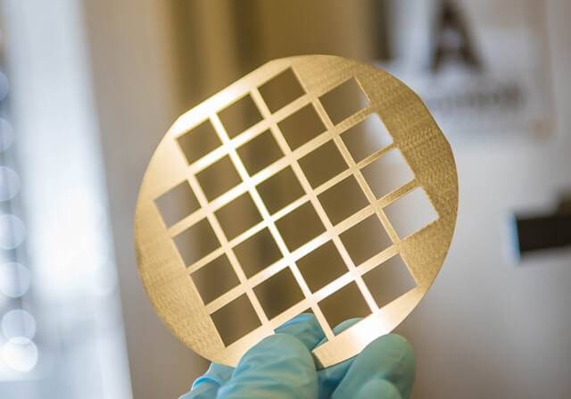
Indium bump bonds are a common way to manufacture 3D flip chip devices for use in superconducting quantum electronics. These devices are manufactured using Angstrom Engineering’s physical vapor deposition systems.
Indium Bump Bonding
This high purity, readily available, and ductile material is suitable for combining Josephson junctions with Al/AlOx/Al architecture onto silicon. As the bumps are more than a few microns in height, high deposition rates are utilized together with high capacity thermal evaporation sources (CH-5 & CH-6) in order to realize suitable throughputs and minimal heat load on the substrate.
Water Cooled Chambers
Angstrom’s chambers are easily fitted with water cooling channels, successfully compensating for the high temperatures essential for suitable indium solder bumps.
Automated Masking
Based on feature size, flip chip bumps can be deposited through shadow masks.